Every modern technology — from smartphones to aircraft and artificial intelligence — depends on one thing: semiconductors.
Often referred to as chips, these are tiny electronic components that serve as the building blocks of digital systems, enabling devices to think, calculate, and communicate.
In 2024, the global semiconductor industry sales reached $630.5 billion. Estimates from the World Semiconductor Trade Statistics (WSTS) project worldwide sales will hit $701 billion in 2025, confirming the scale of an industry now central to global infrastructure.
The OECD describes semiconductors as a foundational technology — comparable to steel in the industrial age or oil in the 20th century.
Today, chips are treated as strategic infrastructure. The U.S., EU, Japan, South Korea, and China are each investing billions to secure supply and build domestic capacity.
This article explains what chips are, how they work, how they evolved, and why manufacturing them has become one of the most complex and strategic industrial challenges of the century.
What Chips Are
A chip is a small electronic component that processes, stores, or directs data within digital devices. It receives input, performs tasks such as calculating, saving, or routing, and sends the results to the next part of the system: a screen, motor, or sensor.
Every chip functions via millions of interconnected electrical paths (switches) that open or close to transmit signals. In basic terms, every digital device — whether it's a car engine or a smartphone — depends on countless yes-or-no decisions that happen millions of times each second.
This is the logic behind computer language: 1s and 0s. Each “1” indicates electricity flows (yes), and each “0” indicates it doesn’t (no). By combining millions of these on-off actions, a chip can process anything from a video to a bank transfer or an AI model.
How Chips Work — From Tubes to Silicon
Before chips existed, early computers in the 1940s used large glass tubes as switches.
Each tube, roughly the size of a light bulb, could only handle one yes/no signal at a time.
A complete machine often contained thousands of tubes, generating massive heat and filling entire rooms to perform basic calculations.
The breakthrough came in the 1950s when engineers discovered that silicon — a solid element derived from sand — was ideal for controlling electrical flow on a tiny, stable surface.
Silicon became the foundation of all modern electronics.
Instead of separate tubes, engineers began building flat silicon plates with microscopic routes for electricity.
Using light and chemical reactions, they drew those paths directly onto the silicon, forming millions of invisible switches in a single plate.
Each switch either allows current to pass or blocks it — like a light switch, but on a microscopic level.
The more switches that fit on the plate, the faster and smarter the chip becomes.
Today, advanced chips can contain over 100 billion switches on a surface smaller than a fingernail.
This discovery did more than transform the field of computing. It also gave its name to the region where the first chip companies emerged — Silicon Valley — which would go on to become the global center of the semiconductor industry and modern technology.
Moore’s Law — The Rule of Doubling
In 1965, Gordon Moore, co-founder of Intel, observed that the number of switches (transistors) on a chip was doubling roughly every two years while costs were falling.
His observation — Moore’s Law — became the guiding principle of the semiconductor industry.
For decades, chipmakers achieved this steady doubling, making computers faster and cheaper with every generation.
But as transistors now approach the atomic scale, sustaining that pace has become extremely expensive. Each new generation costs billions of dollars in research and fabrication.
Scaling Over Time
| Era / Technology | Approx. Switch Count | Size of Device | Typical Power Use |
|---|---|---|---|
| 1940s – Vacuum Tubes | 1,000–10,000 | Room-sized machines | Very high (kilowatts) |
| 1970s – Early Silicon Chips | 10,000–100,000 | Desktop computers | Hundreds of watts |
| 1990s – Microprocessors | 1–10 million | PCs, early phones | Tens of watts |
| 2020s – Advanced AI Chips | 50–100+ billion | Smartphones, AI servers | High (managed via cooling) |
From Processing to Purpose — The Variety of Chips
Not all chips do the same job.
Over time, semiconductors split into specialized categories — each serving a distinct role in modern life.
| Type | Main Function | Used In |
|---|---|---|
| Logic Chips (CPU, GPU, AI processors) | Run software and calculations | Computers, smartphones, data centers |
| Memory Chips (DRAM, NAND) | Store information temporarily or permanently | All digital devices |
| Power & Analog Chips | Manage electricity and signal conversion | Cars, appliances, industrial systems |
| Sensor Chips | Detect motion, light, or pressure | Cameras, vehicles, robotics |
| Communication Chips | Handle connectivity (Wi-Fi, 5G, satellite) | Phones, routers, defense systems |
Each layer supports the digital economy — from computing to manufacturing automation and energy grids.
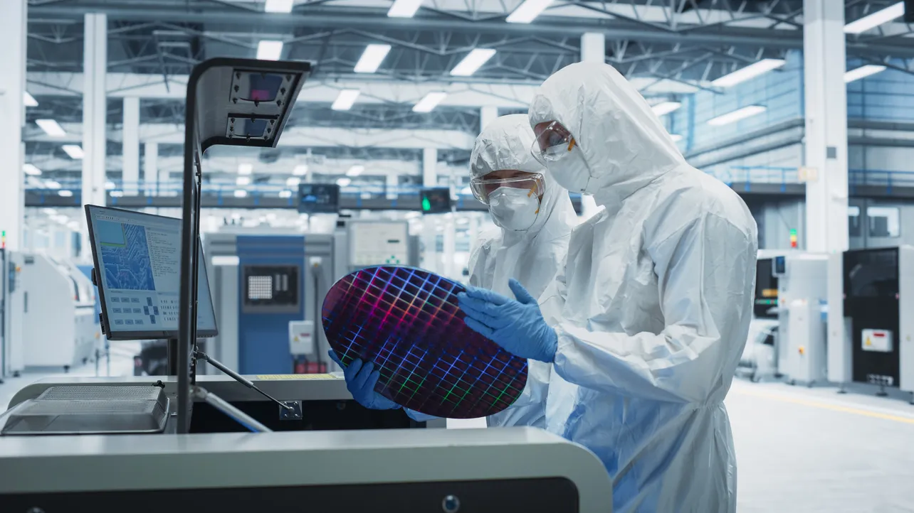
Why Manufacturing Chips Is So Difficult
Producing chips is one of the most complex industrial processes ever created.
Each facility, called a fab (short for fabrication plant), contains hundreds of production tools and thousands of automated steps — all done in sealed, dust-free rooms.
1. Cost and Scale
Building a single advanced fab can cost $20–30 billion, according to McKinsey and SEMI.
That cost comes from:
- Extreme precision machinery, like EUV (Extreme Ultraviolet) lithography tools from ASML, which alone can cost over $200 million per unit.
- Dozens of chemical and plasma steps are repeated across hundreds of wafer layers.
- 24/7 operation — fabs run continuously for months without interruption.
2. Energy and Water Use
A modern fab uses as much electricity as a small city (100–150 MW) and millions of liters of ultra-pure water (UPW) daily.
Water is needed for washing wafers between each step, while electricity powers lasers, pumps, vacuum systems, and temperature control systems-
That’s why major fabs are located near stable grids and abundant water sources — Taiwan’s Hsinchu, Arizona’s desert pipelines, or South Korea’s Pyeongtaek industrial zones.
3. Size and Workforce
A leading-edge fab typically spans 200,000–300,000 square meters, employing 3,000–5,000 engineers and technicians directly.
Each process area must stay 10,000 times cleaner than hospital air.
Even a speck of dust can destroy millions of dollars’ worth of wafers.
4. Supply Chain Complexity
One advanced chip involves over 1,000 separate inputs — from silicon wafers and photoresists to specialty gases like neon and fluorine.
Most are produced by a single or a few suppliers worldwide.
When the war in Ukraine reduced neon output in 2022, chipmakers scrambled to secure alternatives for their lithography systems.
How the Industry Is Structured
Semiconductor production is deeply globalized and highly specialized.
| Stage | Main Task | Leading Regions / Firms |
|---|---|---|
| Design | Define chip architecture and function | United States (NVIDIA, AMD, Apple, Qualcomm) |
| Manufacturing (Foundries) | Fabricate wafers and chips | Taiwan (TSMC), South Korea (Samsung), U.S. (Intel) |
| Equipment & Materials | Machines, wafers, gases, and chemicals | Netherlands (ASML), Japan (Tokyo Electron), U.S. (Applied Materials) |
| Assembly & Testing | Package and verify finished chips | Malaysia, Vietnam, China |
Roughly 70 % of global fabrication capacity is concentrated in East Asia — primarily Taiwan, South Korea, and China.
This regional dominance brings efficiency, but also systemic risk: any disruption in one area can halt global production.
Geopolitics and Industrial Policy
The 2021–22 chip shortage exposed how fragile the system had become.
A few missing microcontrollers stopped global car production.
Governments responded with massive investment programs:
United States – CHIPS and Science Act (2022):
$52 billion in subsidies and tax incentives to build domestic fabs, fund R&D, and train the workforce. Intel, TSMC, and Samsung have all announced major U.S. projects.
European Union – EU Chips Act (2023):
Targeting 20 % of global production by 2030 (up from 8–10 % today). Focus on pilot lines, joint ventures (Intel Magdeburg, STMicro–GlobalFoundries France), and research through IMEC.
Japan and South Korea:
Japan backs Rapidus (an 8-billion-USD state-supported foundry) to rebuild advanced logic capacity, while Korea’s K-Semiconductor Belt expands Samsung and SK hynix facilities with new tax benefits.
China:
Beijing invests over $140 billion in state-backed programs to build self-reliance in mature nodes (28–65 nm), while advancing SMIC and local equipment suppliers despite export controls.
Each bloc is competing for security, not just profit — because every modern weapon, phone, and power grid depends on chips.
Challenges and the Road Ahead
Concentration risk:
East Asia remains the production core. Building redundancy in the U.S. and EU will take years and vast funds.
Rising costs:
The next generation of chips requires sub-nanometer-precision tools and new materials, such as germanium and gallium nitride, each adding to costs and complexity.
Skilled workforce shortage:
McKinsey projects a gap of 300,000 qualified workers by 2030 — mostly process engineers and equipment technicians.
Energy and sustainability:
A single fab’s energy footprint rivals small power plants; manufacturers are under pressure to transition to renewable sources and recycle water.
Fragmentation of standards:
Export controls, competing subsidies, and national security rules risk splitting the once-unified chip ecosystem into regional blocs.
Outlook to 2030
The next decade will define who leads the semiconductor age.
AI servers, electric vehicles, and high-performance computing will drive unprecedented chip demand.
Market projection: WSTS forecasts around $800 billion by 2026, and major consultancies expect up to $1 trillion by 2030.
Manufacturing shift: New fabs are being built in the U.S., EU, Japan, and India — yet Asia will remain dominant through experience, suppliers, and scale.
Technology frontier: The move toward 3D stacking, chiplet design, and advanced packaging allows multiple chips to work together as one — the next evolution beyond transistor density.
Despite rising costs and politics, the fundamentals remain unchanged:
A chip receives data, performs work, and sends results — faster, smaller, and more precisely with each generation.
Conclusion
From glass tubes to atomic-scale silicon, semiconductors have become the nervous system of the modern world.
They define industrial power, military readiness, and digital innovation.
The race to master them is no longer about gadgets — it’s about global balance.
Every byte of the digital age begins and ends with a semiconductor.
Sources
World Semiconductor Trade Statistics (WSTS Fall 2024 Forecast)
OECD Science & Technology Outlook 2024
SEMI Manufacturing & Materials Report 2024
McKinsey Semiconductor Workforce Report 2024
European Commission – EU Chips Act 2023
U.S. Department of Commerce – CHIPS Program 2024
IMEC, TSMC, ASML Investor Data 2024
Reuters, Nikkei Asia, and company filings